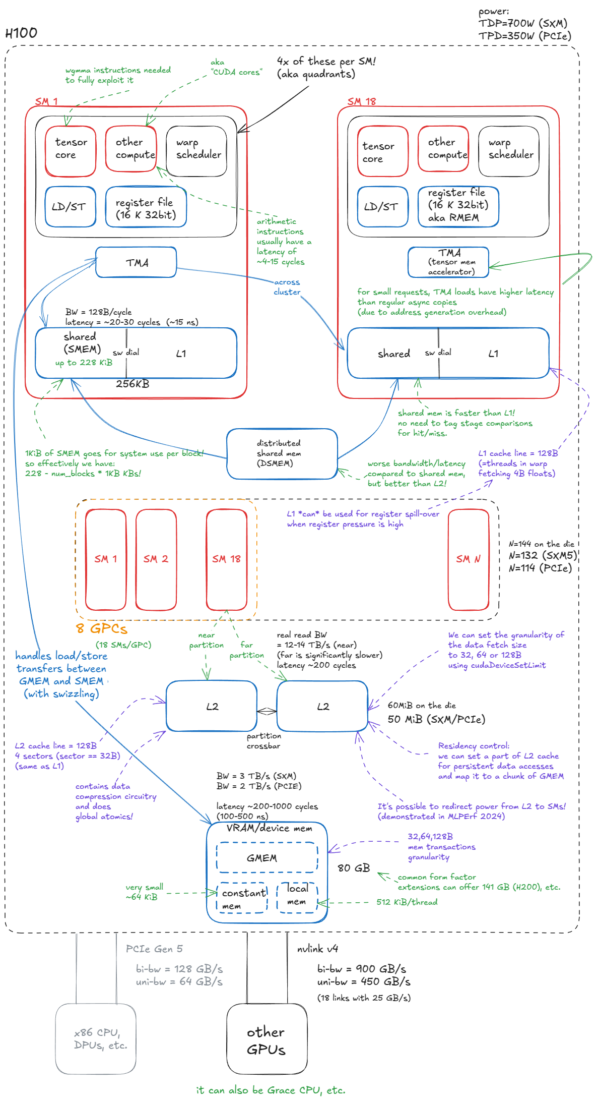
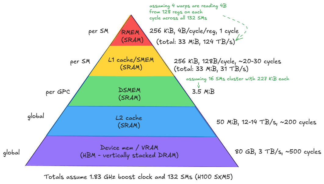
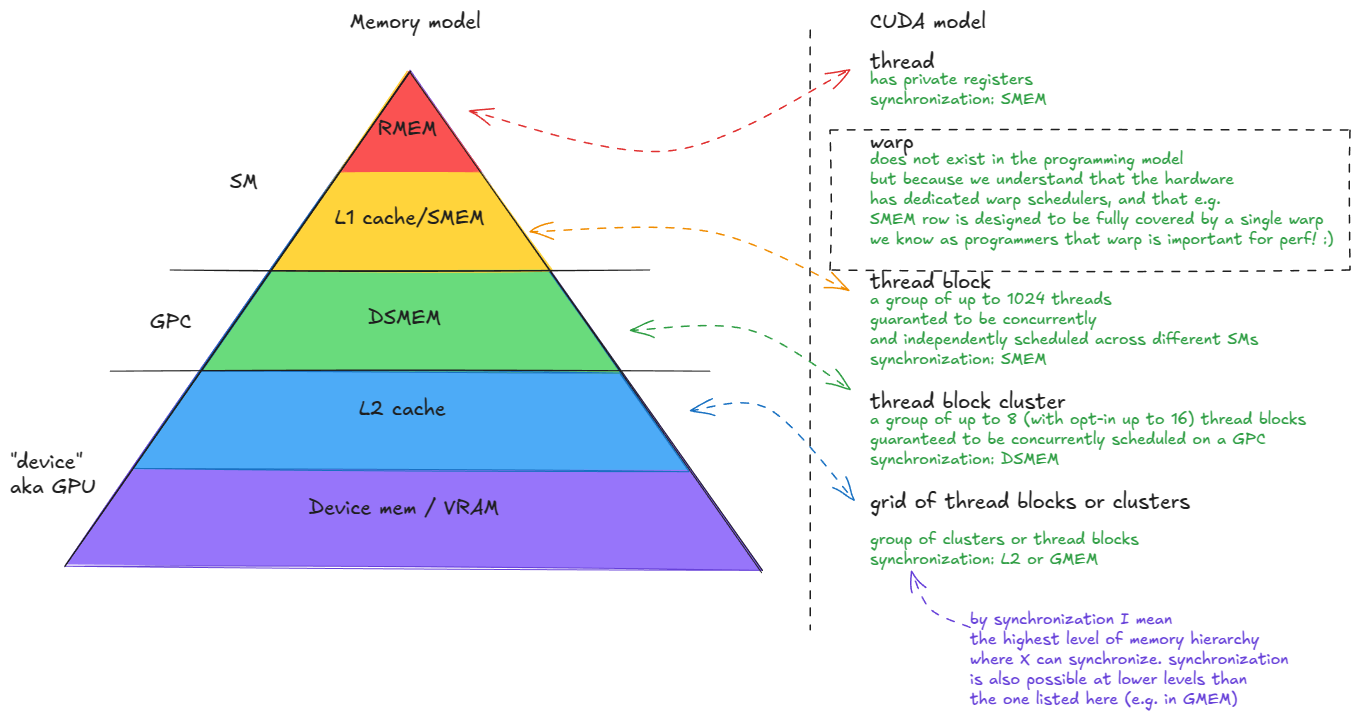
Device memory (VRAM). In CUDA terminology, “device” memory refers to off-chip DRAM—physically separate from the GPU die but packaged together on the same board—implemented as stacked HBM. It hosts global memory (GMEM), per-thread “local” memory (register spill space), etc. ⤴️
L2 cache. A large, k-way set-associative cache built from SRAM. It is physically partitioned into two parts; each SM connects directly to only one partition and indirectly to the other through the crossbar. ⤴️
Distributed shared memory (DSMEM). The pooled shared memories (SMEM) of a physically close group of SMs (a GPC). ⤴️
L1 cache. A smaller, k-way set-associative SRAM cache private to each SM. ⤴️
Shared memory (SMEM). Programmer-managed on-chip memory. SMEM and L1 share the same physical storage, and their relative split can be configured in software. ⤴️
Register file (RMEM). The fastest storage, located next to the compute units. Registers are private to individual threads. Compared to CPUs, GPUs contain far more registers, and the total RMEM capacity is of the same size as the combined L1/SMEM storage. ⤴️
Figure 2: Memory hierarchy of the H100 (SXM5) GPU ⤴️
Moving from device memory down to registers (levels 1-5), you see a clear trend: bandwidth increases by orders of magnitude, while both latency and capacity decrease by similar orders of magnitude. ⤴️
Keep the most frequently accessed data as close as possible to the compute units. ⤴️
Minimize accesses to the lower levels of the hierarchy, especially device memory (GMEM). ⤴️
Tensor Memory Accelerator (TMA), introduced with Hopper. TMA enables asynchronous data transfers between global memory and shared memory, as well as across shared memories within a cluster. ⤴️
compute, the fundamental unit is the streaming multiprocessor (SM)⤴️
SMs are grouped into graphics processing clusters (GPCs): each GPC contains 18 SMs, and there are 8 GPCs on the GPU. Four GPCs connect directly to one L2 partition, and the other four to the second partition. ⤴️
The GPC is also the hardware unit that underpins the thread-block cluster abstraction in CUDA ⤴️
earlier I said each GPC has 18 SMs, so with 8 GPCs we’d expect 144 SMs. But SXM/PCIe form factors expose 132 or 114 SMs. Where’s the discrepancy? It’s because that 18 × 8 layout is true only for the full GH100 die — in actual products, some SMs are fused off. This has direct implications for how we choose cluster configurations when writing kernels. E.g. you can’t use all SMs with clusters spanning more than 2 SMs. ⤴️
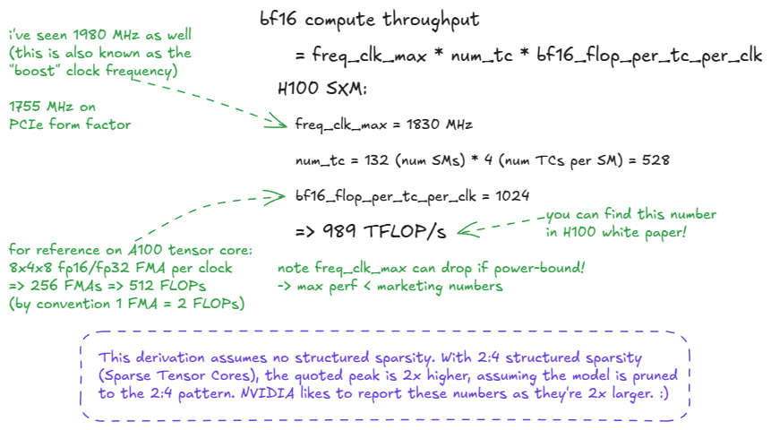
Tensor Cores. Specialized units that execute matrix multiplications on small tiles (e.g., 64x16 @ 16x256) at high throughput. Large matrix multiplications are decomposed into many such tile operations, so leveraging them effectively is critical for reaching peak performance. ⤴️
CUDA cores and SFUs. The so-called “CUDA cores” (marketing speech) execute standard floating-point operations such as FMA (fused multiply-add: c = a * b + c). Special Function Units (SFUs) handle transcendental functions such as sin, cos, exp, log, but also algebraic functions such as sqrt, rsqrt, etc. ⤴️
Load/Store (LD/ST) units. Circuits that service load and store instructions, complementary to the TMA engine. ⤴️
Warp schedulers. Each SM contains schedulers that issue instructions for groups of 32 threads (called warps in CUDA). A warp scheduler can issue one warp instruction per cycle. ⤴️
ie 1 warp = 32 threads = runs in 1 warp scheduler at any point of time
Each SM is physically divided into four quadrants, each housing a subset of the compute units described above. ⤴️
ie each SM has 4 of each
An SM can issue instructions from at most four warps simultaneously (i.e., 128 threads in true parallel execution at a given cycle).
However, an SM can host up to 2048 concurrent threads (64 warps). These warps are resident and scheduled in and out over time, allowing the hardware to hide memory/pipeline latency. ⤴️
simultaneously since 4 quadrants = 4 warp schedulers = 4 x 32 threads = 128 threads
total that can be stored = 64 warps (inclusive of the 4 active warps — ie 16 can be stored per warp scheduler)
The peak throughput is calculated as: perf = freq_clk_max * num_tc * flop_per_tc_per_clk
or in words: maximum clock frequency × number of tensor cores × FLOPs per tensor core per cycle. ⤴️
FLOP/s = a unit of throughput: floating-point operations per second.
FLOPs (with a lowercase s) = the plural of FLOP (operations).
FLOPS (all caps) is often misused to mean throughput, but strictly speaking should only be read as “FLOPs” (the plural of FLOP). FLOPS used as FLOP/s is SLOP! :) ⤴️
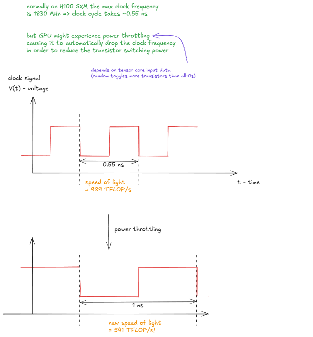
Figure 4: Power throttling reduces clock frequency and lowers the effective “speed of light” ⤴️
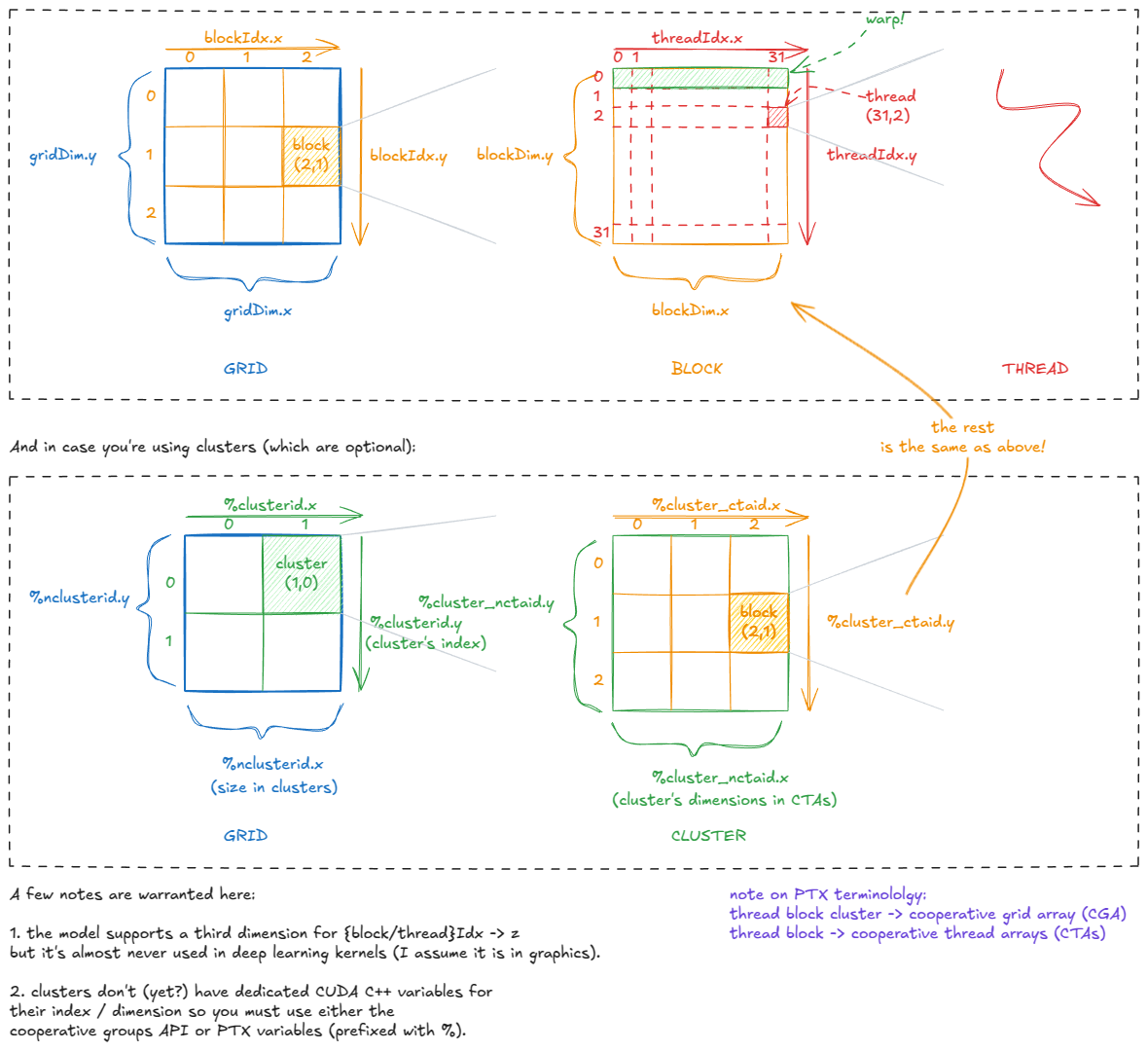
Every thread is “aware” of its position in the CUDA hierarchy through variables such as gridDim, blockIdx, blockDim, and threadIdx. Internally, these are stored in special registers and initialized by the CUDA runtime when a kernel launches. ⤴️
Each thread can then compute its global coordinates, e.g.
const int x = blockIdx.x * blockDim.x + threadIdx.xconst int y = blockIdx.y * blockDim.y + threadIdx.y
and use those to fetch its assigned pixel from global memory (image[x][y]), perform some pointwise operation, and store the result back. ⤴️
Figure 6: CUDA’s built-in variables: how threads know where they are ⤴️
Connecting the CUDA model back to the hardware, one fact should now be clear: a thread block should contain at least 4 warps (i.e., 128 threads).
Why?
A thread block is resident on a single SM.
Each SM has 4 warp schedulers—so to fully utilize the hardware, you don’t want them sitting idle. ⤴️
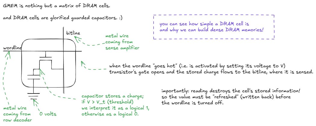
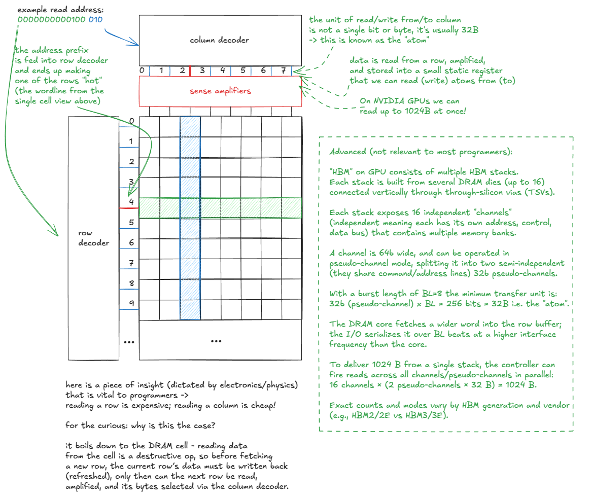
Let’s dive into GMEM. As noted earlier, it is implemented as a stack of DRAM layers with a logic layer at the bottom (HBM). ⤴️
Figure 7: Inside a DRAM cell: transistor + capacitor, wordline + bitline ⤴️
If the matrix in our example were column-major, the situation would flip: elements in a column would be stored contiguously, so the efficient choice would be to traverse rows in the inner loop to avoid the DRAM penalty.
So when people say “GMEM coalescing is very important”, this is what they mean: threads should access contiguous memory locations to minimize the number of DRAM rows touched. ⤴️
Shared memory (SMEM) has very different properties from GMEM. It is built from SRAM cells rather than DRAM, which gives it fundamentally different speed and capacity trade-offs. ⤴️
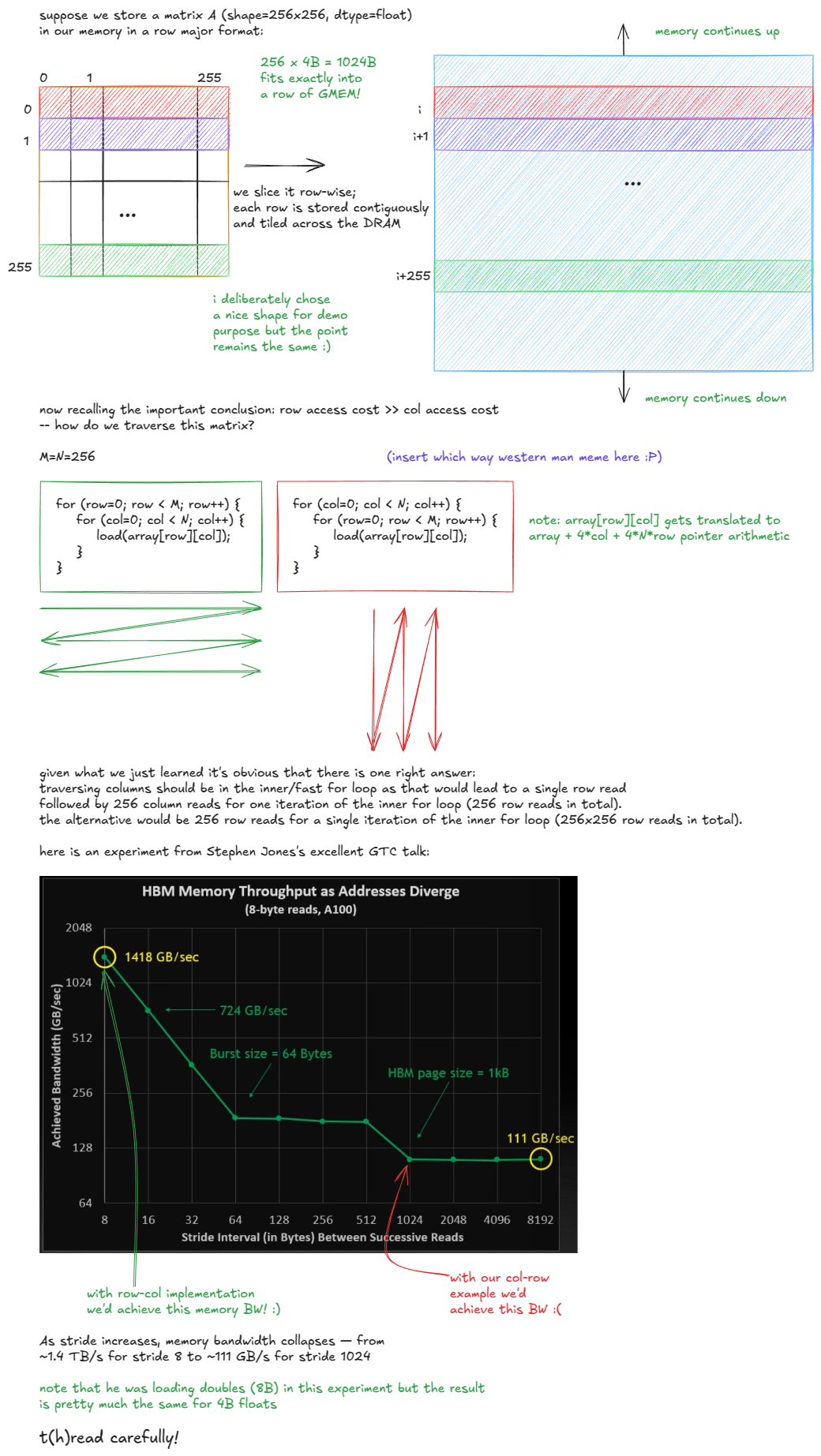
SMEM is organized into 32 banks, each bank 32 bits wide (4 bytes):
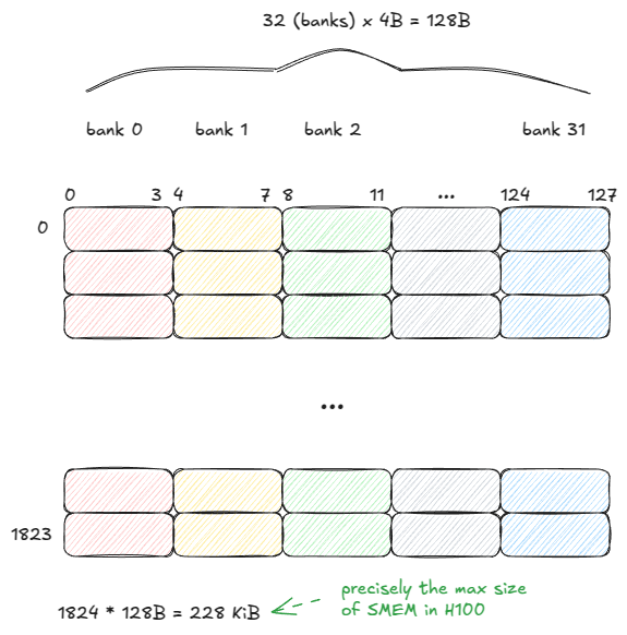
first one with 3-way bank conflict, should this take 4 cycles instead since there is another thread accessing 0,0
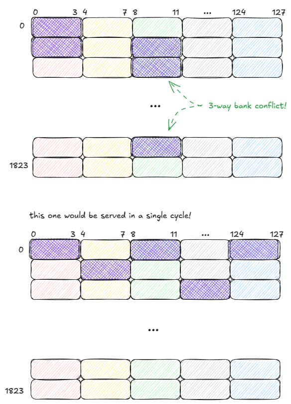
Importantly: if multiple threads in a warp access the same address within a bank, SMEM can broadcast (or multicast) that value to all of them.
In the below example, the request is served in a single cycle:
Bank 1 can multicast a value to 2 threads.
Bank 2 can multicast a value to 3 threads.
Figure 12: SMEM: multicasting (served in a single cycle) ⤴️
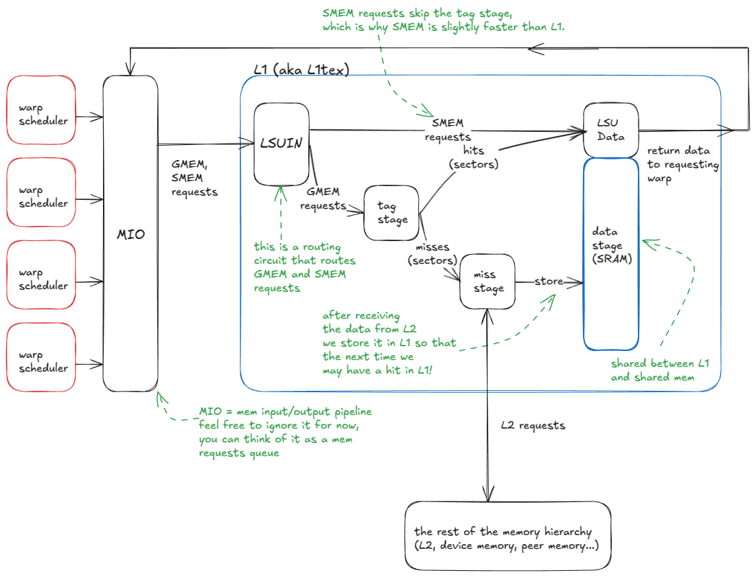
L1 and SMEM share the same physical storage, but L1 adds a hardware-managed scaffolding layer around that storage. ⤴️
the logic flow of the L1 cache is:
A warp issues a memory request (either to SMEM or GMEM).
Requests enter the MIO pipeline and are dispatched to the LSUIN router.
The router directs the request: SMEM accesses are served immediately from the data array, while GMEM accesses move on to the tag-comparison stage.
In the tag stage, the GMEM address tags are compared against those stored in the target set to determine if the data is resident in L1.
On a hit, the request is served directly from the data array (just like SMEM).
On a miss, the request propagates to L2 (and beyond, if necessary, up to GMEM or peer GPU memory). When the data returns, it is cached in L1, evicting an existing line, and in parallel sent back to the requesting warp.
When a GMEM address enters the tag stage, the hit/miss logic unfolds as follows:
The tag stage receives the GMEM address.
The set id bits are extracted, and all cache lines (tags) in that set are checked.
If a tag match is found (potential cache hit):
The line’s validity flags are examined.
* If invalid → it is treated as a cache miss (continue to step 4).
* If valid → the requested sectors are fetched from the data array and delivered to the warp’s registers.
If no match is found (cache miss), the request is routed to the rest of the memory hierarchy (L2 and beyond).
When the data returns from L2, it is stored in the set, evicting an existing line according to the replacement policy (e.g., pseudo-LRU), and in parallel delivered to the requesting warp. ⤴️
this is what L1 cache-misses refers to
L2 is not too dissimilar from L1, except that it is global (vs. per-SM), much larger (with higher associativity), partitioned into two slices connected by a crossbar, and supports more nuanced persistence and caching policies. ⤴️
biggest generational jump so far was from Ampere → Hopper, with the introduction of:
Distributed Shared Memory (DSMEM): direct SM-to-SM communication for loads, stores, and atomics across the SMEMs of an entire GPC.
TMA: hardware unit for asynchronous tensor data movement (GMEM ↔ SMEM, SMEM ↔ SMEM).
Thread Block Clusters: a new CUDA programming model abstraction for grouping blocks across SMs.
Asynchronous transaction barriers: split barriers that count transactions (bytes) instead of just threads. ⤴️
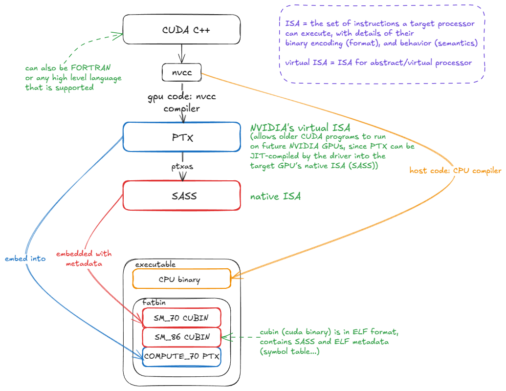
Let’s move one level above the hardware to its ISA (Instruction Set Architecture). An ISA is simply the set of instructions a processor (e.g., an NVIDIA GPU) can execute, along with their binary encodings (opcodes, operands, etc.) and behavioral semantics. Together, these define how programmers can direct the hardware to do useful work.
The human-readable form of an ISA is known as the assembly⤴️
On NVIDIA GPUs, the native ISA is called SASS. Unfortunately, it is poorly documented—especially for the most recent GPU generations. Some older generations have been partially or fully reverse engineered, but official documentation remains limited. ⤴️
PTX is NVIDIA’s virtual ISA: an instruction set for an abstract GPU. PTX code is not executed directly; instead, it is compiled by ptxas into the native ISA (SASS). ⤴️
The key advantage of PTX is forward compatibility. ⤴️
PTX is embedded into the CUDA binary alongside native SASS. When the binary runs on a future GPU, if matching SASS code is not already present, the PTX is JIT-compiled into SASS for the target architecture:
Because this is where the last few percent of performance can be found. On today’s scale, those “few percent” are massive: if you’re training an LLM across 30,000 H100s, improving a core kernel’s performance by even 1% translates into millions of dollars saved. ⤴️
there are likely no new asymptotic complexity classes waiting to be discovered — the big wins are (mostly) gone. But squeezing out ~1% efficiency across millions of GPUs is the equivalent of saving a few SMRs (small modular reactors) worth of energy. ⤴️
when writing CUDA C++ you want to stay tightly coupled to the compiler’s output (PTX/SASS). This lets you double-check that your hints (e.g., #pragma unroll to unroll a loop, or vectorized loads) are actually being lowered into the expected instructions (e.g., LDG.128). ⤴️
Note also that some instructions have no equivalent in CUDA C++; you simply have to write inline PTX! ⤴️
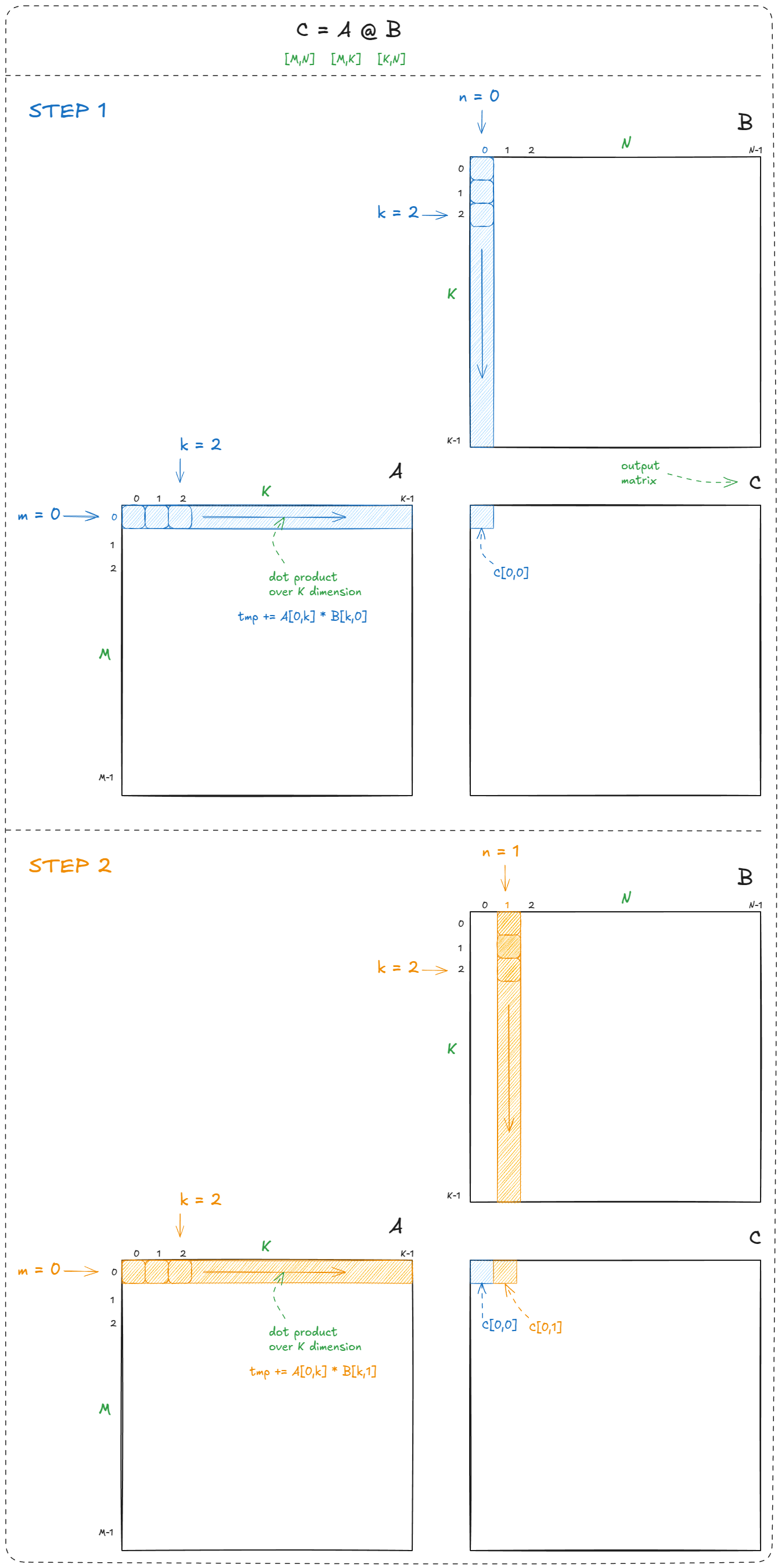
We loop over the rows (m) and columns (n) of the output matrix (C), and at each location compute a dot product (C[m,n] = dot(a[m,k],b[k,n])). This is the textbook definition of matmul:
Figure 16: Naive CPU matmul example
In total, matrix multiplication requires M × N dot products. Each dot product performs K multiply-adds, so the total work is 2 × M × N × K FLOPs (factor of 2 because, by convention, we count FMA = multiply + add). ⤴️
C = alpha * A @ B + beta * C. This is the classic GEMM (General Matrix Multiply). Setting alpha = 1.0 and beta = 1.0 recovers the simpler C = A @ B. ⤴️
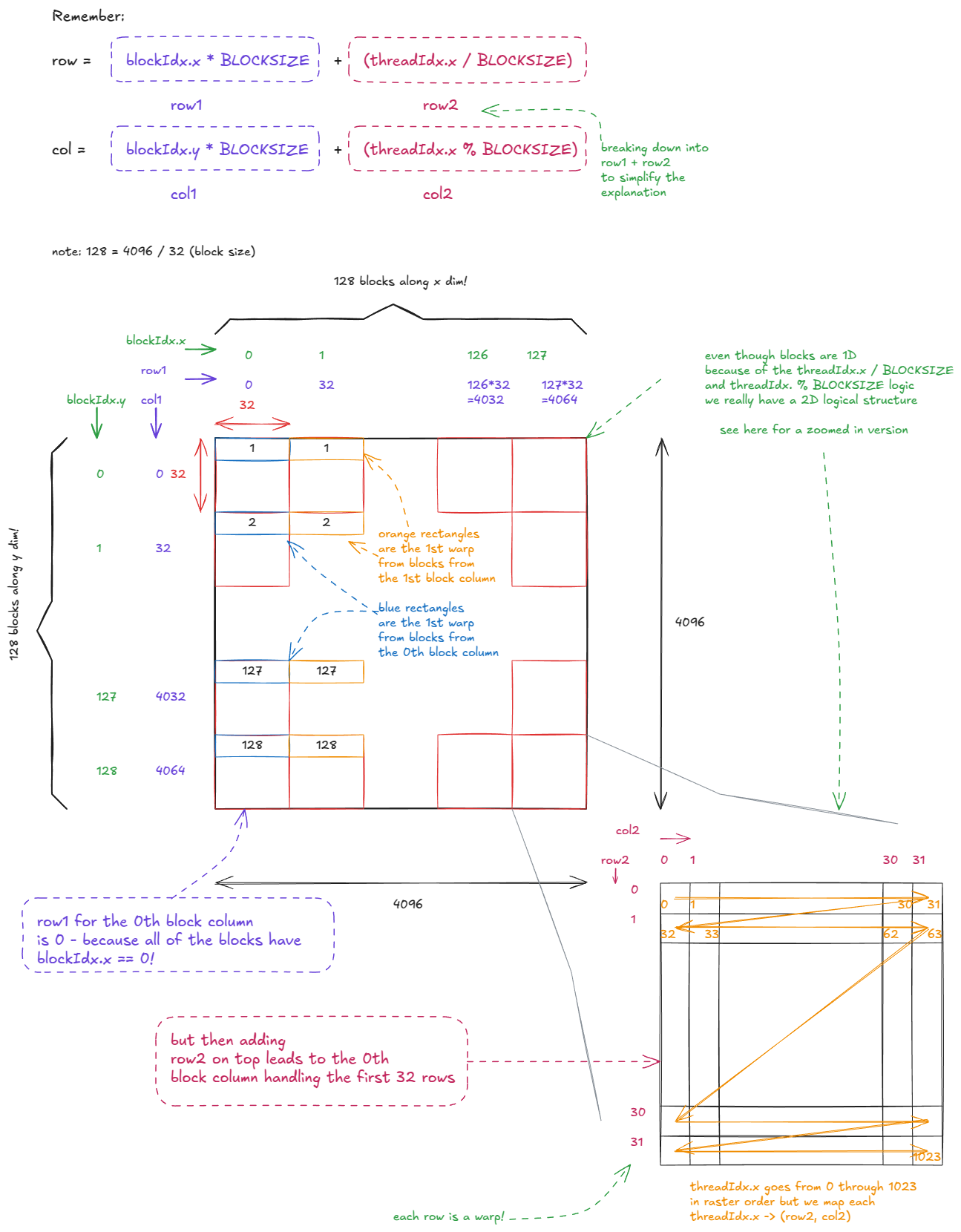
Kernels are written from the perspective of a single thread. This follows the SIMT (Single Instruction, Multiple Threads) model: the programmer writes one thread’s work, while CUDA handles the launch and initialization of grids, clusters, and blocks. (Other programming models, such as OpenAI’s Triton[22], let you write from the perspective of a tile instead.)
Each thread uses its block and thread indices (the variables we discussed earlier) to compute its (row, col) coordinates in C and write out the corresponding dot product.
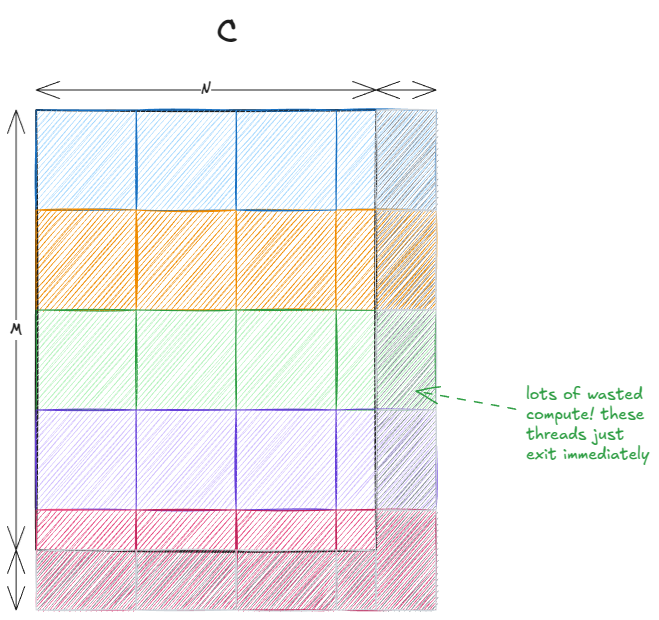
We tile the output matrix using as many 32×32 thread blocks (1024 threads) as possible.
If M or N are not divisible by 32, some threads fall outside the valid output region of C. That’s why we include a guard in the code.
The last two points combined lead to a phenomenon commonly known as the tile quantization: